How Should I Route SPI Lines? Expert Tips for Optimal PCB Design! Our top 10 pcb routing tips
If you are searching about [PCB design] Layout for SPI bus due to ringing - PCBWay you've came to the right place. We have 25 Images about [PCB design] Layout for SPI bus due to ringing - PCBWay like First 4-Layer PCB: SPI Testing with DSO - Misconfigured SPI Lines or, First 4-Layer PCB: SPI Testing with DSO - Misconfigured SPI Lines or and also 7 tips for high-speed PCB-routing design. Read more:
[PCB Design] Layout For SPI Bus Due To Ringing - PCBWay
![[PCB design] Layout for SPI bus due to ringing - PCBWay](https://pcbwayfile.s3-us-west-2.amazonaws.com/project/22/01/27/2355323170760.png) www.pcbway.com
www.pcbway.com
[PCB design] Layout for SPI bus due to ringing - PCBWay
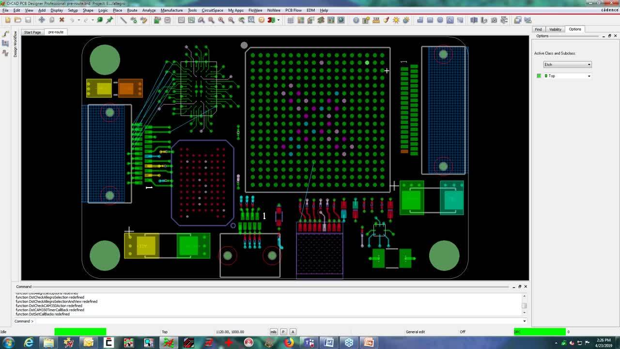
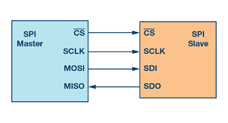
Pcb Design - PCB Routing Of SPI Lines - Electrical Engineering Stack
 electronics.stackexchange.com
pcb design - PCB routing of SPI lines - Electrical Engineering Stack ...
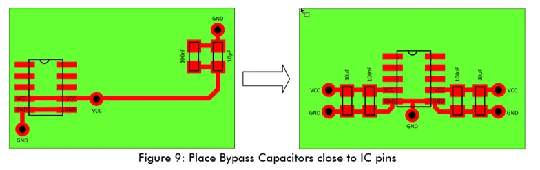
Your Route To Design Success: PCB Routing Tips From The Pros | EMA
 www.ema-eda.com
Your Route to Design Success: PCB Routing Tips from the Pros | EMA ...
Angled Vs. Curved Routing In PCB Design Specifically For SPI
 electronics.stackexchange.com
Angled vs. curved routing in PCB design specifically for SPI ...
First 4-Layer PCB: SPI Testing With DSO - Misconfigured SPI Lines Or
 electronics.stackexchange.com
First 4-Layer PCB: SPI Testing with DSO - Misconfigured SPI Lines or ...
7 Tips For High-speed PCB-routing Design
 www.pcbgogo.com
7 tips for high-speed PCB-routing design
7 Tips For High-speed PCB-routing Design
 www.pcbgogo.com
7 tips for high-speed PCB-routing design
First 4-Layer PCB: SPI Testing With DSO - Misconfigured SPI Lines Or
 electronics.stackexchange.com
First 4-Layer PCB: SPI Testing with DSO - Misconfigured SPI Lines or ...
PCB Design Archives - Page 4 Of 5 - Microcontroller Tips
 www.microcontrollertips.com
PCB Design Archives - Page 4 of 5 - Microcontroller Tips
Pcb Routing Guidelines Pcb Design Guidelines For Freshers Types | Hot
 www.hotzxgirl.com
Pcb Routing Guidelines Pcb Design Guidelines For Freshers Types | Hot ...
7 Tips For High-speed PCB-routing Design
 www.pcbgogo.com
7 tips for high-speed PCB-routing design
High Speed PCB Layouts: Routing Tips - Porticos | Product Design
 www.porticos.net
High Speed PCB Layouts: Routing Tips - Porticos | Product Design ...
7 Tips For High-speed PCB-routing Design
 www.pcbgogo.com
7 tips for high-speed PCB-routing design
First 4-Layer PCB: SPI Testing With DSO - Misconfigured SPI Lines Or
 electronics.stackexchange.com
First 4-Layer PCB: SPI Testing with DSO - Misconfigured SPI Lines or ...
7 Tips For High-speed PCB-routing Design
 www.pcbgogo.com
7 tips for high-speed PCB-routing design
7 Tips For High-speed PCB-routing Design
 www.pcbgogo.com
7 tips for high-speed PCB-routing design
High-Speed PCB Design Tips And Guidelines | Phil's Lab | Altium Designer
 resources.altium.com
High-Speed PCB Design Tips and Guidelines | Phil's Lab | Altium Designer
7 Tips For High-speed PCB-routing Design
 www.pcbgogo.com
7 tips for high-speed PCB-routing design
Our Top 10 PCB Routing Tips
 www.proto-electronics.com
Our Top 10 PCB Routing Tips
Tips For High Speed PCB Routing With An Ease And Simple Process
 www.crimpcircuits.com
Tips for high speed PCB routing with an ease and simple process
Pcb Design - PCB Routing Of SPI Lines - Electrical Engineering Stack
 electronics.stackexchange.com
pcb design - PCB routing of SPI lines - Electrical Engineering Stack ...
7 Tips For High-speed PCB-routing Design
 www.pcbgogo.com
7 tips for high-speed PCB-routing design
Tips For High Speed PCB Routing With An Ease And Simple Process
 www.crimpcircuits.com
Tips for high speed PCB routing with an ease and simple process
[PCB Design] Layout For SPI Bus Due To Ringing - PCBWay
![[PCB design] Layout for SPI bus due to ringing - PCBWay](https://pcbwayfile.s3-us-west-2.amazonaws.com/project/22/01/27/2353442548018.png) www.pcbway.com
www.pcbway.com
[PCB design] Layout for SPI bus due to ringing - PCBWay
7 Tips For High-speed PCB-routing Design
 www.pcbgogo.com
7 tips for high-speed PCB-routing design
High speed pcb layouts: routing tips. pcb routing guidelines pcb design guidelines for freshers types. 7 tips for high-speed pcb-routing design