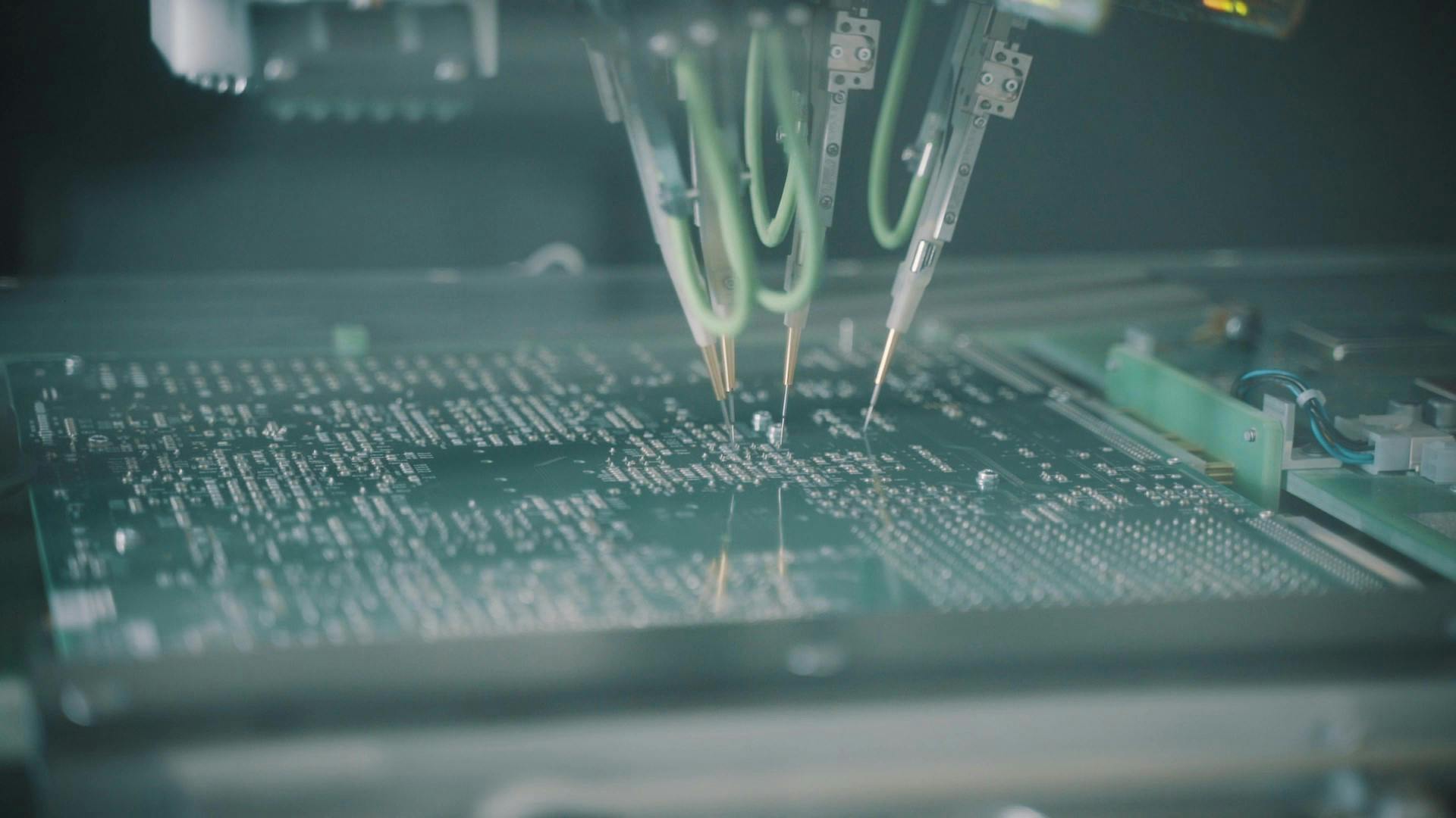
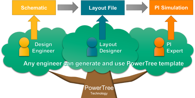
Streamline Your PCB Design Process: The Key to Efficiency! streamline your pcb design flow with in-design and post-route power ...
If you are searching about Optimizing PCB layout for assembly and manufacturing efficiency you've visit to the right place. We have 25 Pics about Optimizing PCB layout for assembly and manufacturing efficiency like PCB Design Process Improvement: Improving Efficiency and Quality, Streamline Your PCB Design Flow with In-Design and Post-Route Power and also PCB Process Flow Chart | www.homillux.com. Here it is:
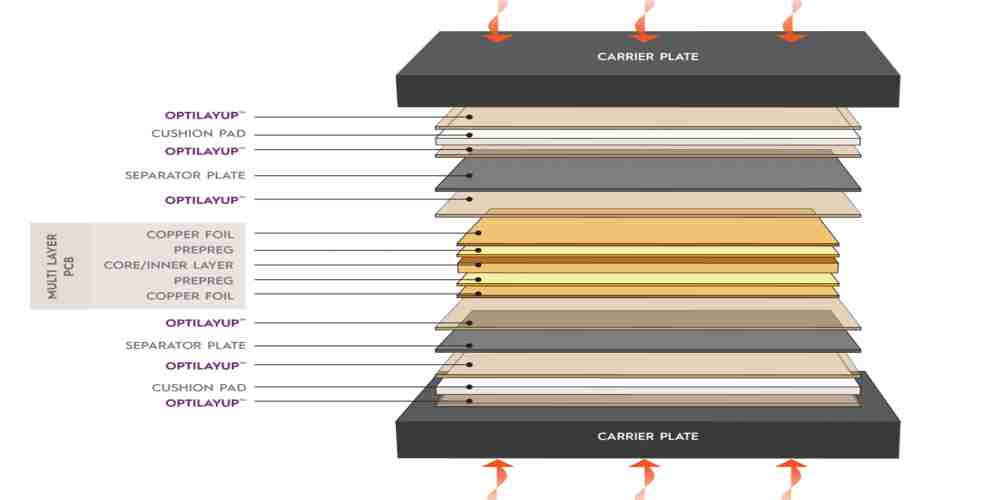
Optimizing PCB Layout For Assembly And Manufacturing Efficiency
 microcad3d.com
Optimizing PCB layout for assembly and manufacturing efficiency
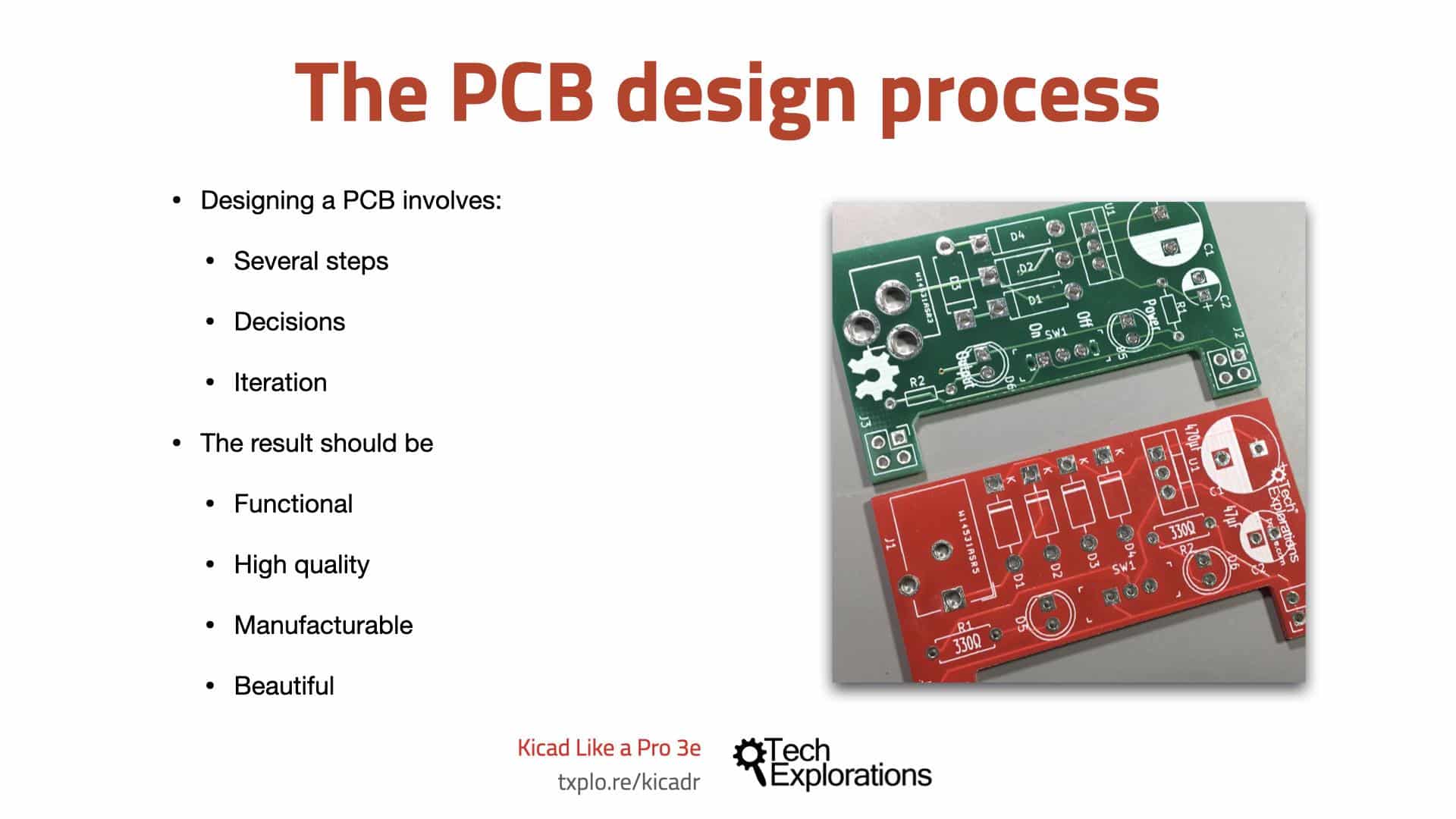
The PCB Design Process, An Overview Of The Necessary Steps
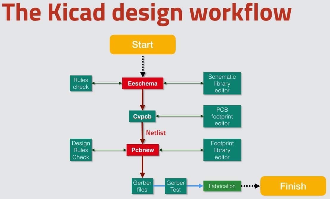 techexplorations.com
The PCB design process, an overview of the necessary steps
The PCB Design Process For Advanced Electronics | Northwest Engineering
 www.nwengineeringllc.com
The PCB Design Process For Advanced Electronics | Northwest Engineering ...
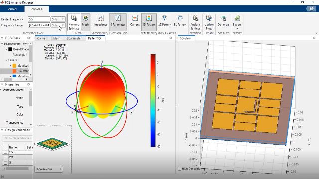
How To Design PCB Antenna - RayPCB
 www.raypcb.com
How to Design PCB Antenna - RayPCB
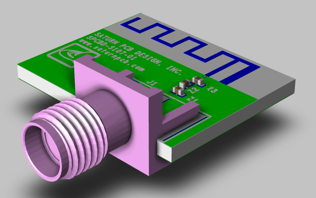
How To Design And Simulate PCB Antenna
 courses.fedevel.com
How to Design and Simulate PCB Antenna
Streamline Your PCB Design Flow With In-Design And Post-Route Power
 community.cadence.com
Streamline Your PCB Design Flow with In-Design and Post-Route Power ...
PCB Design Process Improvement: Improving Efficiency And Quality
 www.01pcb.com
PCB Design Process Improvement: Improving Efficiency and Quality
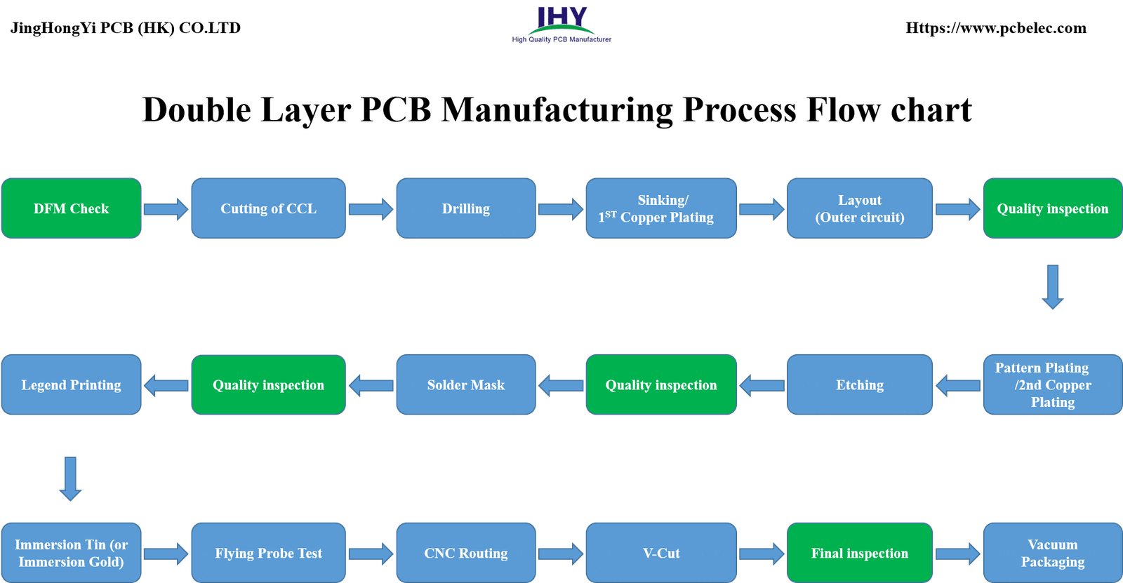
PCB Process Flow Chart | Www.homillux.com
 www.homillux.com
PCB Process Flow Chart | www.homillux.com
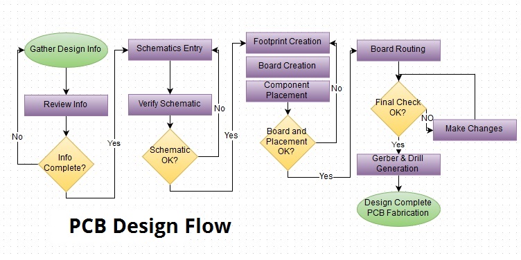
Pcb Design Process Flow - Design Talk
 design.udlvirtual.edu.pe
Pcb Design Process Flow - Design Talk
Maximizing PCB Layout For Testability & Manufacturing Efficiency
 webinars.sw.siemens.com
Maximizing PCB Layout for Testability & Manufacturing Efficiency ...
The Importance Of Design For Manufacturability In PCB Design
 blogs.sw.siemens.com
The importance of Design for Manufacturability in PCB design ...
Design Keyboard PCB: A Comprehensive Guide - MorePCB
 morepcb.com
Design Keyboard PCB: A Comprehensive Guide - MorePCB
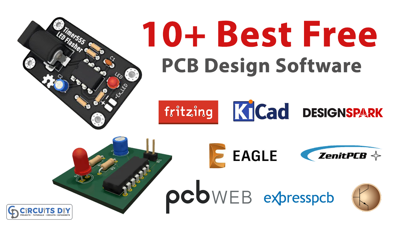
Pcb Software
 www.circuits-diy.com
pcb software
Basic Steps To Design A PCB Layout – PCB HERO
 www.pcb-hero.com
Basic Steps to Design a PCB Layout – PCB HERO
ATE PCB Design: Tips And Best Practices For Optimal Testing Efficiency
 hillmancurtis.com
ATE PCB Design: Tips and Best Practices for Optimal Testing Efficiency ...
PCB Assembly Process Flowchart - Electronics Tutorial | The Best
 www.electronicsandyou.com
PCB Assembly Process Flowchart - Electronics Tutorial | The Best ...
Tech Explorations - KiCad 6 Guide Series - The PCB Design Process
 techexplorations.com
Tech Explorations - KiCad 6 Guide Series - The PCB design process
How To Streamline PCB Assembly Operations With Valor Process
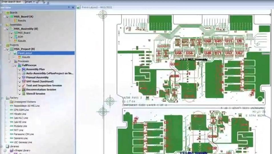 www.mentor.com
How to Streamline PCB Assembly Operations with Valor Process ...
Streamline Your PCB Design Flow With In-Design And Post-Route Power
 community.cadence.com
Streamline Your PCB Design Flow with In-Design and Post-Route Power ...
PCB Design Services | PCB Design Process | PCB Prototyping Process
 arshon.com
PCB Design Services | PCB design Process | PCB Prototyping Process
Pcb Design Process Flow At Louise Whipple Blog
 storage.googleapis.com
Pcb Design Process Flow at Louise Whipple blog
High Performance Pcb Antenna Pcb Antenna Design 41 Of - Vrogue.co
 www.vrogue.co
High Performance Pcb Antenna Pcb Antenna Design 41 Of - vrogue.co
PCB Process Flow Chart | Www.homillux.com
 www.homillux.com
PCB Process Flow Chart | www.homillux.com
SECO: Streamlining The PCB Design Process With SECO
 www.seco.com
SECO: Streamlining the PCB Design Process with SECO
How To Design A PCB Antenna?
 www.nextpcb.com
How to Design a PCB Antenna?
Pcb process flow chart. How to design pcb antenna. Tech explorations